Advanced Integration
Lead Selenide Infrared Sensing Technology

Private Fundraise
This company may be interested in raising funds from accredited investors. You must Request Access to see more information about this company.
Request Access 9


Advanced Integration, Inc. has developed a breakthrough process and technology that will spur rapid advancements in an enormous range of markets and industries.
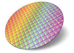
AI has developed a proven high volume manufacturing technique for a Lead Selenide (PbSe) film which adheres directly to silicon -- a groundbreaking development that will have a transformational effect on a array of technologies and products throughout both the photoconductive and photovoltaic markets. This will replace the exsisting methods which do not adhere directly to silicon, provides low-yields, prevents film property enhancements, restricts device design capablities and is difficult for application to possibly increase solar and thermal power generation efficiencies.
AI's semiconductor process development and equipment expertise provides patent-pending technologies to the expanding infrared sensor market -- forecasted as a $100B+ market -- and has huge implications for thermal imaging, sensors, and renewable energy markets and potentially increase efficiencies in the solar technologies.


Lead Selenide (PbSe) materials have been utilized for over 50 years for their ability to detect an infrared response in a spectral range that is increasingly in demand for monitoring modern technologies. While the PbSe materials do conduct at room temperature, making them widely favored in a variety of industries, scientists have been unable to adhere them to anything other than glass without a buffer layer being used. For over half a century no one has been able to provide the necessary semi-conductor device structure to process and manufacture these devices in a cost-effective manner.
Advanced Integration has, for the first time in this technology arena's history, created the solutions necessary for a repeatable, high yield manufacturing process, improved performance, overcoming the issue of adhering PbSe films to silicon and allows widely accpeted design and manufacturing methods to be used.
 AI's semiconductor process and equipment understanding not only enables us to provide PbSe film on silicon, thereby increasing photoconductive and photovoltaic properties, but also improves its infrared performance and provides improves yields. The ability to deposit the PbSe film directly on to silicon instead of glass can reduce the manufacturing costs of the device from $2,000 to $3,000 down to $200 -- a stunning breakthrough in and of itself.
AI's breakthrough technologies can deliver quantum leaps in both performance and cost savings, allowing our 900+ customer base to dramatically increase their sales by both drastically reducing present manufacturing costs as well as providing new and innovative applications, solutions and opening the landscape to allow for the development of new inventions.

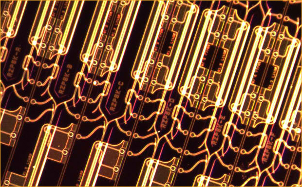
AI has drastically streamlined the process of applying PbSe to materials, while simultaneously creating the first technology enabling it to directlyadhere to silicon without a buffer layer. This opens up an enormous array of applications. Our process uses Sputtering Deposition, and has been granted 3 patents.
The laws of Physics dictate that only certain elements respond to the infrared spectrum, and then to only a certain portion of the spectrum. Our strategic advantage lies in the fact that PbSe's infrared properties respond to the portion of the infrared spectrum that is of major importance to an wide array of commercial markets, as well as military technologies and solar technologies

AI has created the technology, equipment and processes necessary to impact incredible change in a wide variety of markets. Below, just a few of the advantages to our products and services, as well as their potential applications.
 Our PbSe film technology does not require a buffer layer.
We have developed a proven high volume manufacturing technique.
Our process results in lower manufacturing costs and higher production yields.
Sensors can have increased performance.
Our ablility to provide a P-N junction, a feature that potentially increases the
efficiency of solar and thermal energy technology applications.
Our technology can be used to create focal plane arrays, improving
imaging processes.
Allow greater device design capablities.
Advanced Integration will sell equipment and licensing opportunities for our patented technology to companies and provide a coating services for customers. Presently we are not considering supplying sensors or power generation devices to clients. Our products and services will increase efficiency and innovation across innumerable markets, a few of which have been listed below.

Numerous diverse and defensive military innovations or enhancements will be achievable, including improved night vision capabilities, geophysical as well as maritime surveillance, body-heat detection for search and rescue operations. All of these advancements equate to improvements in counter-terrorism and piracy applications.
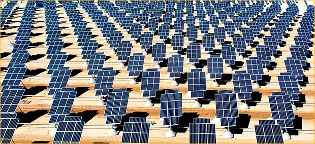
Solar Enhancements
To power every home, solar must become economically viable versus conventional forms of electricity. That is the next major trend in the making. The solar industry as yet, in its infancy is still prohibitively expensive as a capital investment. Total return on investments can still take decades.
To accelerate this new mega-trend, solar energy needs improved performance and to render it totally ubiquitous in every household. Advanced Integration technology will assist in providing solutions this problem, having developed ground breaking technologies and solutions, to improve conversion of solar power to electricity via the co-efficient via the enhanced transmission of electrical energy and conductivity of all solar cells, through their proprietary P-N junction PbSe film, that can improve electrical output possibly even on cloudy days. This is the big problem with solar cells today: Inefficent transmission or conductivity that inhibits the transfer of clean, higher powered electrical output. Advanced Integration's patented solutions to this problem are innovative and quite revolutionary. The global market is so vast, AI foresees solar cell enhancements as a transformational business, with multi-billion dollar potential.


Looking to the future, Advanced Integration, Inc. will build upon the massive potential of our technology and services to further expand our customer base and impact great change across markets. As developing the only large volume manufacturing process for PbSe-silicon sensors and P-N junctions, we have made great strides in the technology. To date, we have obtained 3 patents and 2 additional are pending. We are already working in conjunction with two multi-billion dollar companies to further develop our PbSe films for commercial markets, military markets, power generation, and expect to expand our reach into a broad range of additional markets in the coming years.
Request Additional Information